- 您现在的位置:买卖IC网 > Sheet目录3874 > DSPIC30F2012T-20I/ML (Microchip Technology)IC DSPIC MCU/DSP 12K 28QFN
dsPIC30F Flash Programming Specification
DS70102K-page 58
2010 Microchip Technology Inc.
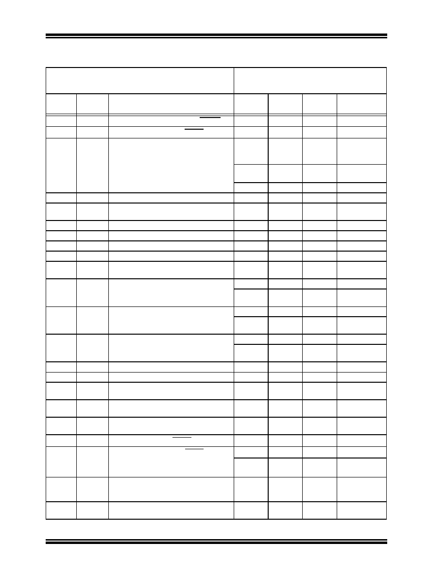
13.0 AC/DC CHARACTERISTICS AND TIMING REQUIREMENTS
TABLE 13-1:
AC/DC CHARACTERISTICS
Standard Operating Conditions
(unless otherwise stated)
Operating Temperature: 25
° C is recommended
Param.
No.
Sym
Characteristic
Min
Max
Units
Conditions
D110
VIHH
High Programming Voltage on MCLR/VPP
9.00
13.25
V
—
D112
IPP
Programming Current on MCLR/VPP
—300
μA—
D113
IDDP
Supply Current during programming
—
30
mA
Row Erase
Program
memory
—
30
mA
Row Erase
Data EEPROM
—
30
mA
Bulk Erase
D001
VDD
Supply voltage
2.5
5.5
V
—
D002
VDDBULK Supply voltage for Bulk Erase
programming
4.5
5.5
V
—
D031
VIL
Input Low Voltage
VSS
0.2 VSS
V—
D041
VIH
Input High Voltage
0.8 VDD
VDD
V—
D080
VOL
Output Low Voltage
—
0.6
V
IOL = 8.5 mA
D090
VOH
Output High Voltage
VDD - 0.7
—
V
IOH = -3.0 mA
D012
CIO
Capacitive Loading on I/O Pin (PGD)
—
50
pF
To meet AC
specifications
P1
TSCLK
Serial Clock (PGC) period
50
—
ns
ICSP mode
1—
μs
Enhanced
ICSP mode
P1a
TSCLKL
Serial Clock (PGC) low time
20
—
ns
ICSP mode
400
—
ns
Enhanced
ICSP mode
P1b
TSCLKH
Serial Clock (PGC) high time
20
—
ns
ICSP mode
400
—
ns
Enhanced
ICSP mode
P2
TSET1
Input Data Setup Timer to PGC
↓
15
—
ns
—
P3
THLD1
Input Data Hold Time from PGC
↓
15
—
ns
—
P4
TDLY1
Delay between 4-bit command and
command operand
20
—
ns
—
P4a
TDLY1a
Delay between 4-bit command operand
and next 4-bit command
20
—
ns
—
P5
TDLY2
Delay between last PGC
↓of command to
first PGC
↑ of VISI output
20
—
ns
—
P6
TSET2VDD
↑ setup time to MCLR/VPP
100
—
ns
—
P7
THLD2
Input data hold time from MCLR/VPP
↑
2—
μs
ICSP mode
5
—
ms
Enhanced
ICSP mode
P8
TDLY3
Delay between last PGC
↓ of command
word to PGD driven
↑ by programming
executive
20
—
μs—
P9a
TDLY4
Programming Executive Command
processing time
10
—
μs—
发布紧急采购,3分钟左右您将得到回复。
相关PDF资料
PIC18LF6310T-I/PT
IC PIC MCU FLASH 4KX16 64TQFP
PIC16LF76T-I/SOG
IC MCU FLASH 8KX14 28SOIC
PIC16F690-I/P
IC PIC MCU FLASH 4KX14 20DIP
PIC16LF74T-I/PTG
IC MCU FLASH 4KX14 44TQFP
DSPIC30F2012T-20I/SO
IC DSPIC MCU/DSP 12K 28SOIC
DSPIC30F3012T-20I/ML
IC DSPIC MCU/DSP 24K 44QFN
DSPIC30F3012T-20I/SO
IC DSPIC MCU/DSP 24K 18SOIC
PIC16F747-E/ML
IC PIC MCU FLASH 4KX14 44QFN
相关代理商/技术参数
DSPIC30F2012T-20I/SO
功能描述:IC DSPIC MCU/DSP 12K 28SOIC RoHS:是 类别:集成电路 (IC) >> 嵌入式 - 微控制器, 系列:dsPIC™ 30F 产品培训模块:XLP Deep Sleep Mode
8-bit PIC® Microcontroller Portfolio 标准包装:22 系列:PIC® XLP™ 18F 核心处理器:PIC 芯体尺寸:8-位 速度:48MHz 连通性:I²C,SPI,UART/USART,USB 外围设备:欠压检测/复位,POR,PWM,WDT 输入/输出数:14 程序存储器容量:8KB(4K x 16) 程序存储器类型:闪存 EEPROM 大小:256 x 8 RAM 容量:512 x 8 电压 - 电源 (Vcc/Vdd):1.8 V ~ 5.5 V 数据转换器:A/D 11x10b 振荡器型:内部 工作温度:-40°C ~ 85°C 封装/外壳:20-DIP(0.300",7.62mm) 包装:管件 产品目录页面:642 (CN2011-ZH PDF) 配用:DV164126-ND - KIT DEVELOPMENT USB W/PICKIT 2DM164127-ND - KIT DEVELOPMENT USB 18F14/13K50AC164112-ND - VOLTAGE LIMITER MPLAB ICD2 VPP
dsPIC30F2012T-30I/ML
功能描述:数字信号处理器和控制器 - DSP, DSC 28LD 30MIPS 12 KB RoHS:否 制造商:Microchip Technology 核心:dsPIC 数据总线宽度:16 bit 程序存储器大小:16 KB 数据 RAM 大小:2 KB 最大时钟频率:40 MHz 可编程输入/输出端数量:35 定时器数量:3 设备每秒兆指令数:50 MIPs 工作电源电压:3.3 V 最大工作温度:+ 85 C 封装 / 箱体:TQFP-44 安装风格:SMD/SMT
dsPIC30F2012T-30I/SO
功能描述:数字信号处理器和控制器 - DSP, DSC 28LD 30MIPS 12 KB RoHS:否 制造商:Microchip Technology 核心:dsPIC 数据总线宽度:16 bit 程序存储器大小:16 KB 数据 RAM 大小:2 KB 最大时钟频率:40 MHz 可编程输入/输出端数量:35 定时器数量:3 设备每秒兆指令数:50 MIPs 工作电源电压:3.3 V 最大工作温度:+ 85 C 封装 / 箱体:TQFP-44 安装风格:SMD/SMT
DSPIC30F2013AT-20E
制造商:MICROCHIP 制造商全称:Microchip Technology 功能描述:High-Performance, 16-bit Digital Signal Controllers
DSPIC30F2013AT-20E/PF-ES
制造商:MICROCHIP 制造商全称:Microchip Technology 功能描述:General Purpose and Sensor Families High-Performance Digital Signal Controllers
DSPIC30F2013AT-20E/PT-ES
制造商:MICROCHIP 制造商全称:Microchip Technology 功能描述:General Purpose and Sensor Families High-Performance Digital Signal Controllers
DSPIC30F2013AT-20EML-ES
制造商:MICROCHIP 制造商全称:Microchip Technology 功能描述:High-Performance Digital Signal Controllers
DSPIC30F2013AT-20EP-ES
制造商:MICROCHIP 制造商全称:Microchip Technology 功能描述:High-Performance Digital Signal Controllers